

Silicon Drift Detectors

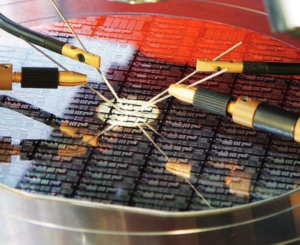
Radiation detectors based on semiconductor materials are nowadays popular choices in several fields of science and industry, due to some unique properties that make them the optimal solution for the detection of photons from the soft-X, up to the Gamma energy range. In their development, Semiconductor Radiation Detectors (SRD) greatly benefited from the maturity of the planar process used in the microelectronics technology
industry, which allowed in 1979 the realization by Josef Kemmer of the first silicon radiation detectors with low leakage currents, that could be adopted for imaging and spectroscopic purposes even at room temperature.
In 1984 Emilio Gatti and Pavel Rehak proposed an ingenious charge transport mechanism for a new type of Si detectors which took the name of semiconductor drift chambers or Silicon Drift Detectors (SDD); these detectors allowed to obtain the same spatial resolution of microstrip detectors using a much reduced number of preamplifiers, and showed an architecture which could make the detector’s capacitance independent of the detector’s active area, with an unprecedented improvement in the noise performance of semiconductor detectors.
SDDs are currently a golden standard for high-resolution spectroscopy applications, even though they are still topic for research and development for the improvmenet of performances, especially in pixelated architectures with large active area.
Wide Bandgap Semiconductor Detectors
While silicon is undoubtedly the most established semiconductor material to convert radiation into electrical signals, its relatively low atomic number and material density makes it unsuitable for the type of application where higher energy photons must be detected in a relatively small thickness. Its relatively low energy bandgap makes it also less appealing for applications where optimal energy resolution must be achieved at room temperature. For this and other reasons, different semiconductor materials, commonly referred to as “wide bandgap” (like GaAs, SiC, CdTe and CdZnTe) are nowadays a relevant research topic.
Unlike silicon, which features a simpler molecular structure and takes advantage of a mature industrial manufacturing process resulting in high crystal purity, wide bandgap materials cannot so far be grown with the same level of purity. Therefore, their greater sensitivity to higher energy radiation and good spectroscopic resolution at room temperature is usually traded-off with inferior charge transport properties and instability in detector performance due to defect in their crystal structure.
Research efforts in the study and characterization of this kind of complex detectors currently center around their performance degradation in high-rate conditions, i.e., when a high dose of radiation is impinging on the device in a short time. A phenomenon commonly referred to has high flux polarization.